A quick history and presentation of a custom-built digital signal processing platform. Equipped with a dual-core Cortex-A7 CPU and 1 GB of DDR3L RAM it allows for experimenting with advanced audio effects in real time. Bare metal firmware guarantees low latency (<1 ms digital, <3 ms end-to-end). Multiple audio in/outs, expansion ports as well as a rich user interface ensure high degree of usability in real life situations.
Context
Wanting to be able to make my own guitar effects was what got me into electronics. At first I was copying freely available classics but my long term goal was to be able to make a reverb. That is how my longest-running project has started -- the Audio DSP Platform. From circa 2018 I have been playing around with designing my own audio DSP boxes -- I am on the fourth hardware iteration right now. While having to design both hardware and software slows down the development significantly, there is no bigger satisfaction than holding something you have created in hand.
Previous Iterations
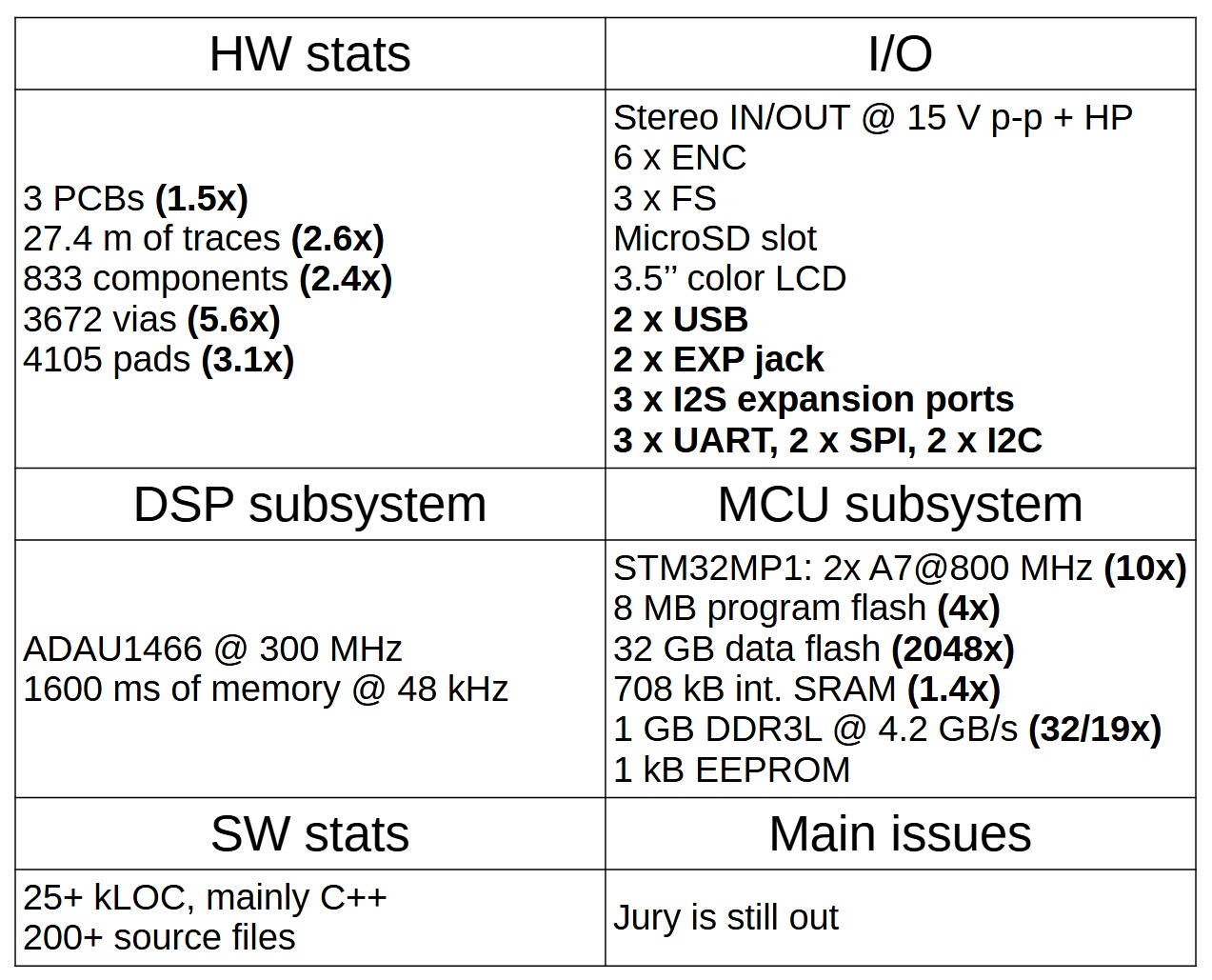
As mentioned before, the subject of this article is the fourth iteration of my DSP platform. In this section I will quickly summarize my previous attempts while pointing out the shortfalls of each edition. Each subsection will be accompanied by a summary table that will illustrate exponential growth in complexity by comparing a few key metrics. Values written in bold highlight main changes compared to the previous version.
First Attempt -- ADAU1701 and ATMega328PB in an 1590B Enclosure (Q1 2019)
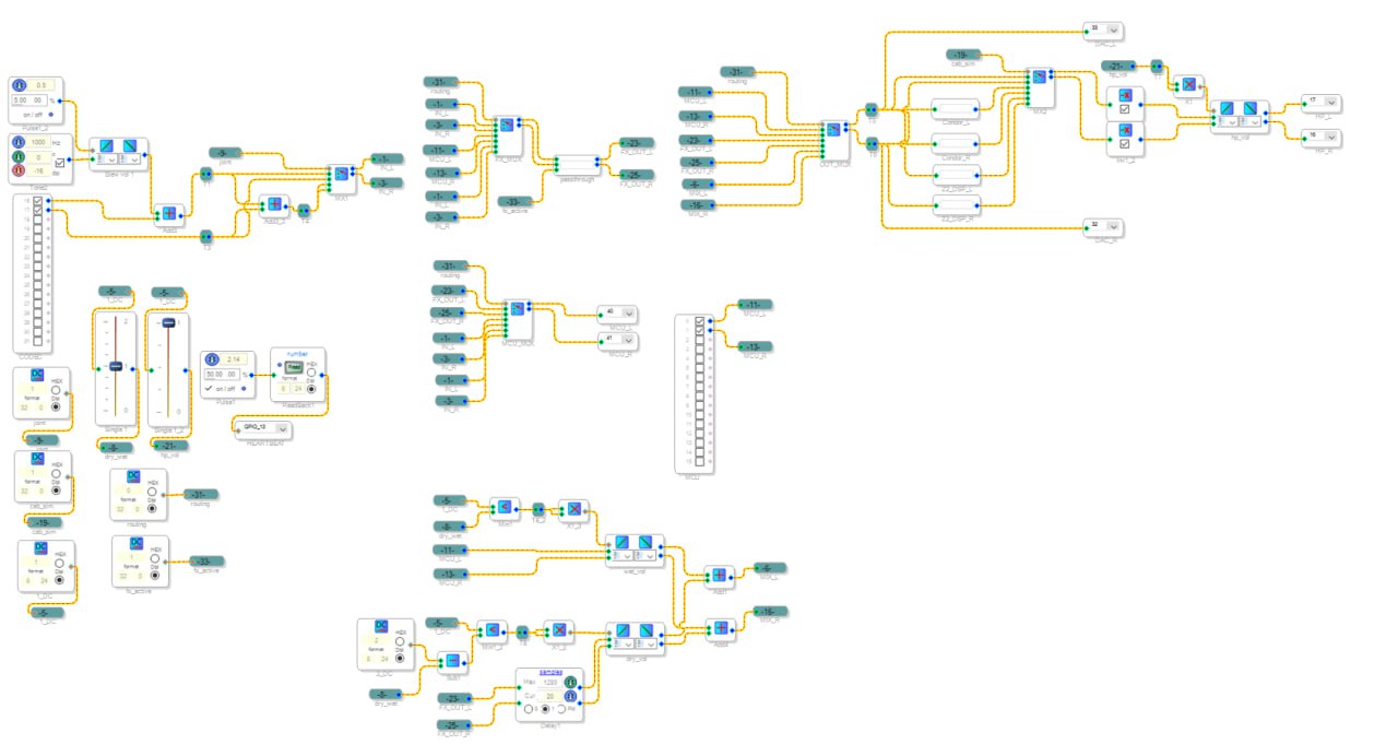
Let me start by introducing one of the rare constant characteristics of this project -- each iteration is fitted with an Analog Devices DSP from the SigmaDSP product line. What drew me to it is also one of its limiting factors -- the only way to program it is through a graphical interface where you assemble the algorithm from a predefined set of blocks (see below). I chose to start this way as the only MCUs I knew how to use were AVRs, I did not have any DSP coding experience and development tool cost for 'big boy' DSPs was prohibitive. Oh well, you have to start somewhere.
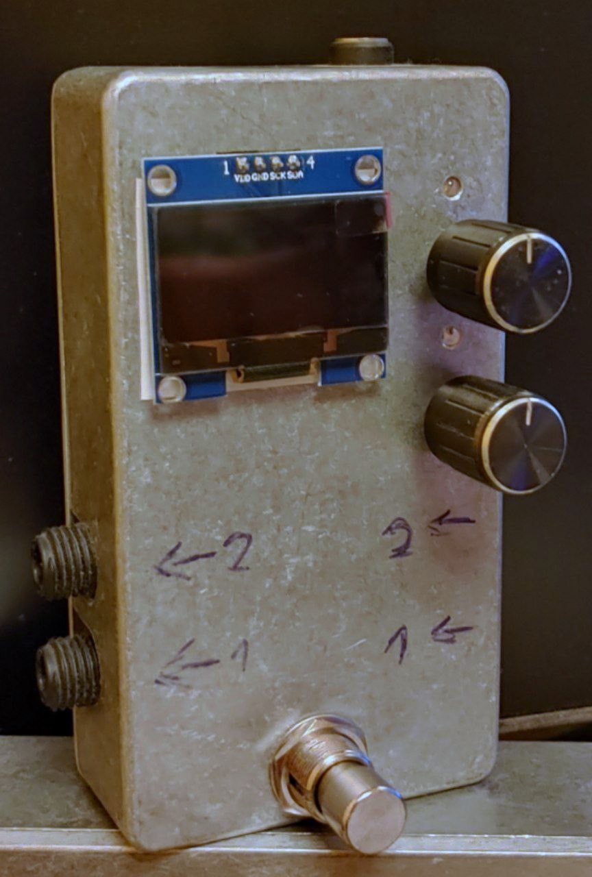
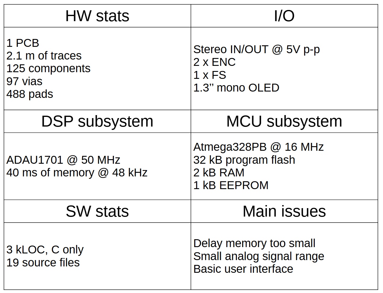
The first iteration of this project was also the first device that was developed by me from start to finish. I decided to use a compact Hammond 1590B case as I was already familiar with this format from my stompbox-copying days. ADAU1701 served as an integrated DSP+CODEC combo while ATmega328PB took care of the user interface and system management. This project was used mostly to familiarize myself with the hardware development process as ADAU1701 was too memory-constrained to be useful for reverbs (only 40 ms @ 48 kHz).
Second Attempt -- ADAU1452 and ATMega324PB in an 1590XX Enclosure (Q4 2019)
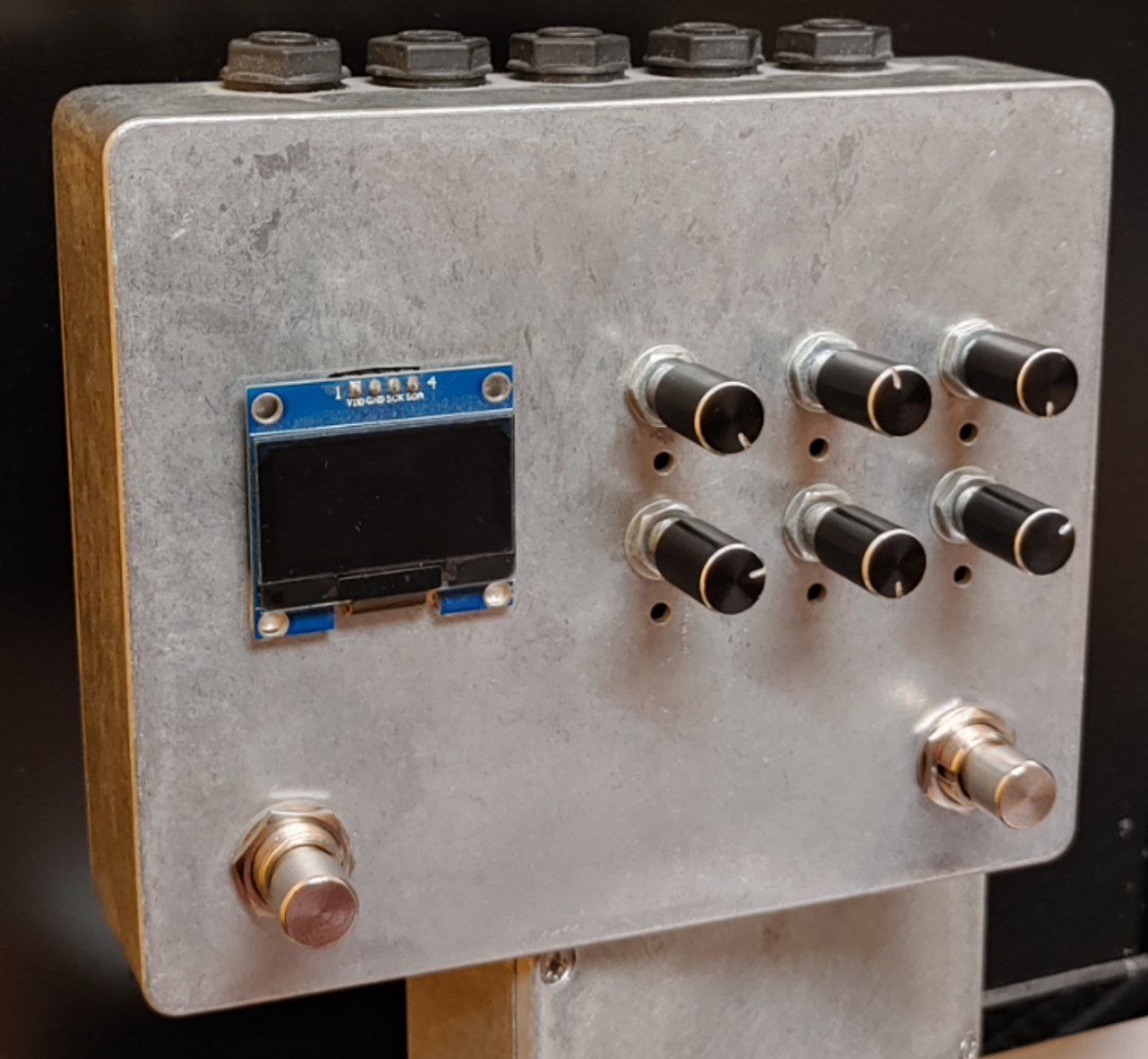
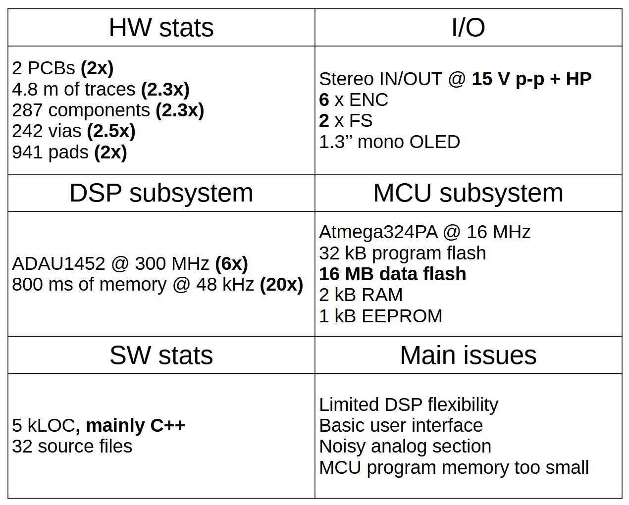
The second attempt used the ADAU1701's much bigger brother -- the ADAU1452. Not only did it boast a 6x increase in clockspeed, but more importantly -- 20x increase in memory. With 800 ms of delay memory available I was finally be able to experiment with algorithmic reverb. Other system improvements included bigger Hammond 1590XX enclosure, expanded I/O as well as 15 Vp-p audio I/O for use in hot amplifier FX loops. This iteration's biggest shortfall was the noisy analog section. While it was OK in an FX loop, it was unusable in front of a high-gain amplifier or a stompbox.
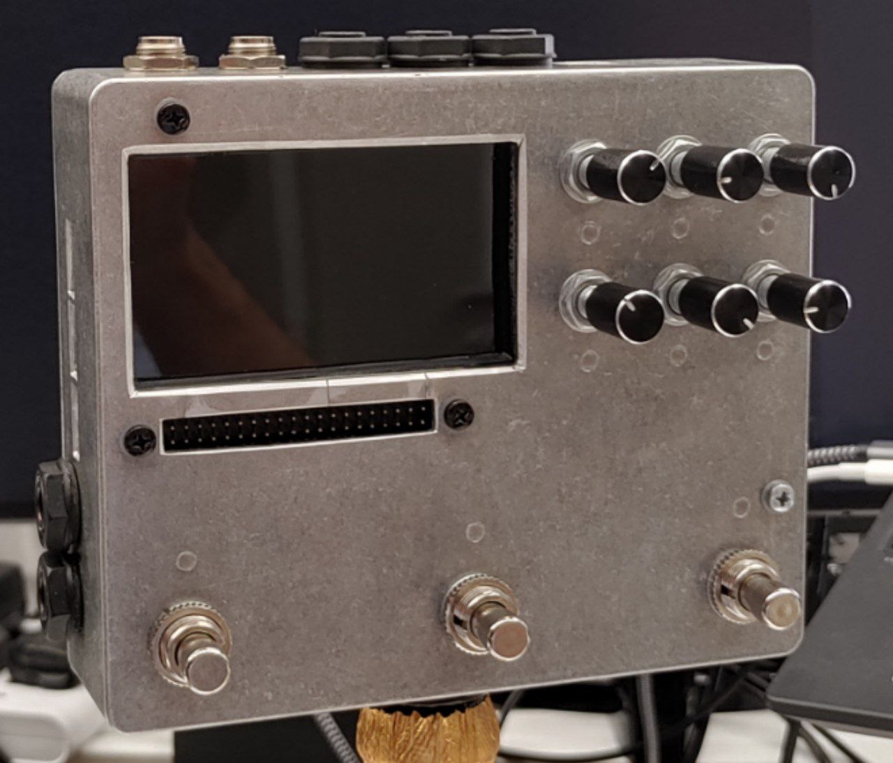
Third Attempt -- ADAU1466 and STM32F765 in an 1590XX Enclosure (Q4 2020)
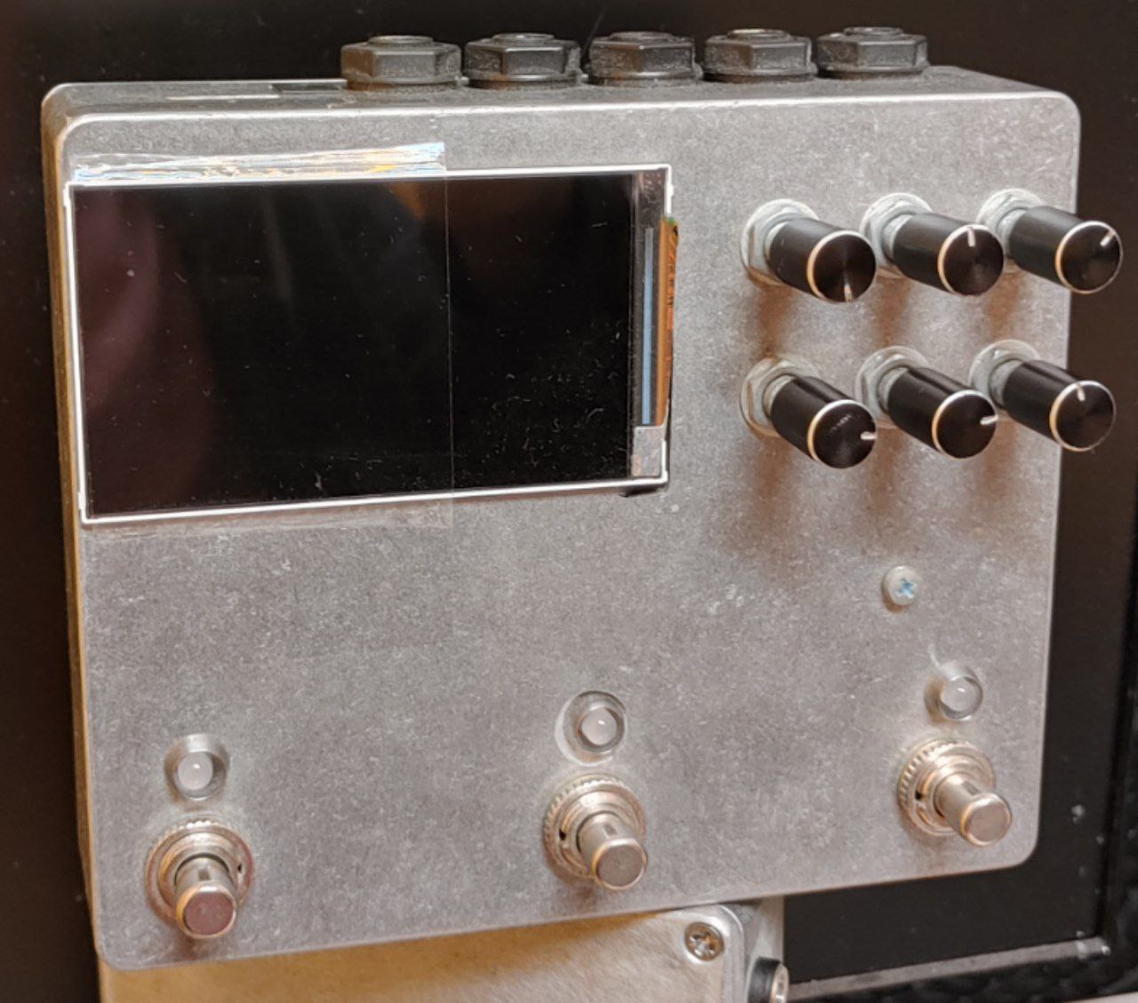
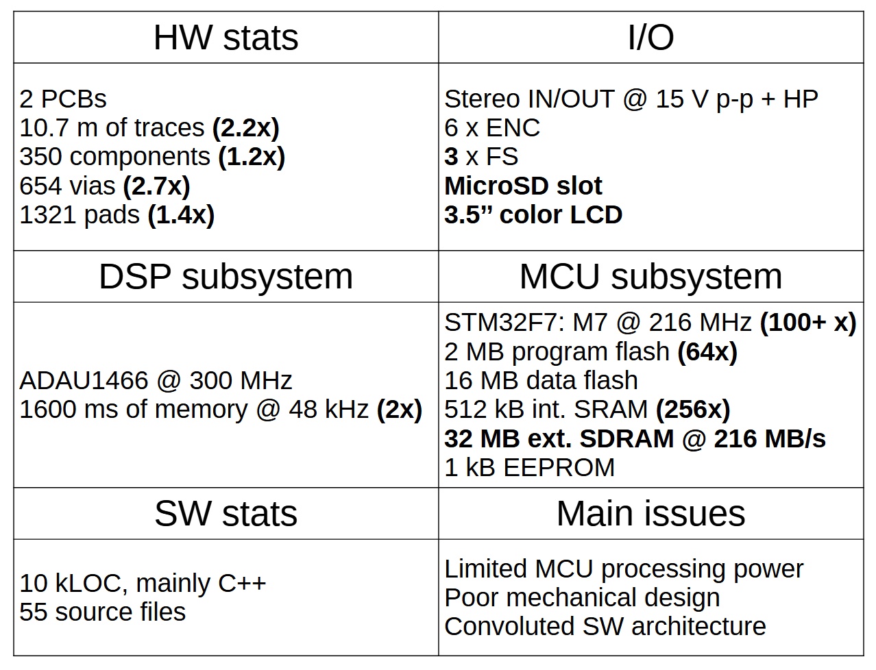
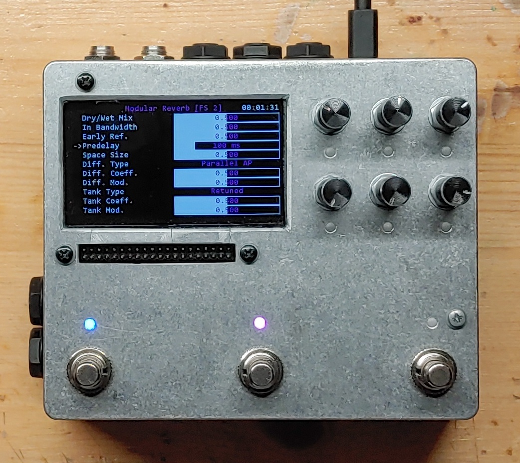
Somewhere along the way I became frustrated with SigmaStudio's limiting graphical environment. That has pushed me towards processing audio on MCUs. The STM32F765 became my choice due to fairly beefy 216 MHz Cortex-M7 core as well as rich documentation and community support. Extensive reverse engineering work by Andy Brown allowed me to use a high quality display from a Sony Ericsson Vivaz U5i for a crisp user interface. I/O was also expanded by an additional footswitch as well as a MicroSD card slot. As I still was not confident in my C++ DSP skills, the ADAU-family device was here to stay.
Intro and Specs
After having built the third version I have decided to put this project on pause. It was time for me to focus on my engineering and masters theses. I have also took up a position of a lead embedded engineer in an university motorcycle racing team (LEM Wroclaw Motorsport -- check them out!). Sometime close to my graduation I managed to find a job in embedded systems so this has further contributed to my lack of leftover creative energy. Having said that -- I started work on the fourth iteration sometime in late 2022.
This almost two year-long hiatus had its advantages too -- I have gained a substantial amount of experience that allowed me to make a significant leap in hardware complexity while making the system more elegant and extensible. The star of the show is (then) newly unveiled STM32MP157 microprocessor. Compared to ST's line of microcontrollers, it offers an order of magnitude jump in CPU and memory capabilities while keeping a familiar peripheral collection -- essentially an MCU on steroids. The other big change was the I/O system enriched with digital audio and general-purpose interfaces.
System Architecture
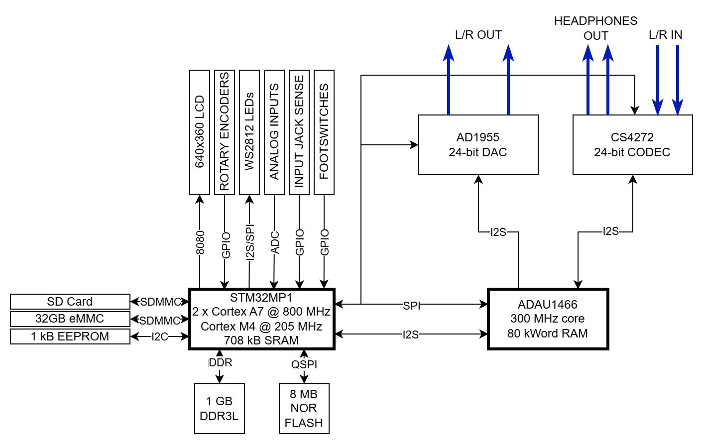
While the system diagram is fairly self-explanatory, let me justify some of my choices:
- The ADAU1466 DSP is still included despite the fact that this platform's main focus is the STM32MP1 MPU. One reason is that I wanted to preserve backwards compatibility with my previously created effects. The other, more important one, is that this arrangement allows me to take advantage of two unique ADAU's features:
- Single sample latency processing (MPU is block-based)
- Built-in ASRCs to allow for a multirate system without software resampling (e.g. latency-critical processing at 96 kHz on ADAU and a reverb on MPU at 48 kHz)
- AD1955 DAC for the lowest possible noise floor on main audio outputs. The second iteration has caused me to overcorrect in the DAC department and I am positive that the AD1955 is overkill but hey, if it ain't broke -- don't fix it.
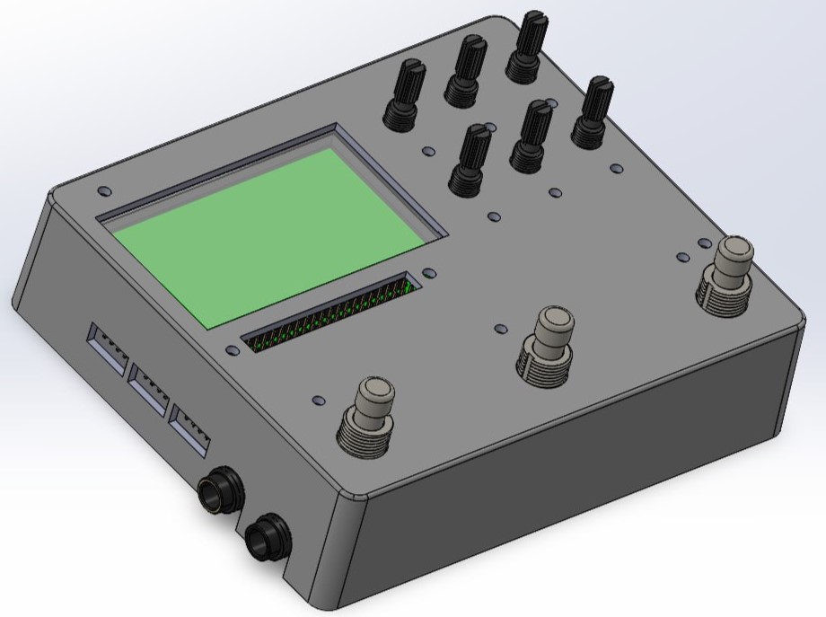
Mechanical Design
Up to this iteration, the mechanical constraints were fairly loose. I just employed the 'pray that it fits' strategy. While it has always fit eventually, the outcome was not that great, especially with the third edition where I managed to break multiple LCDs during assembly.
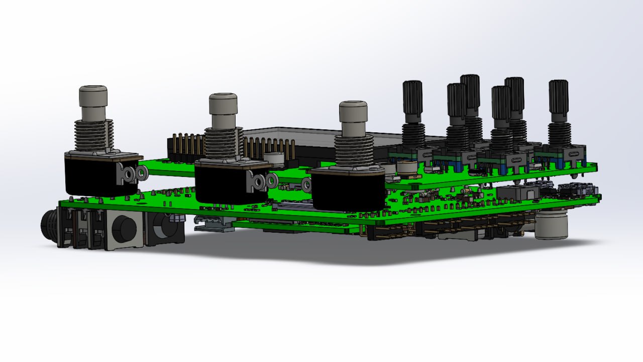
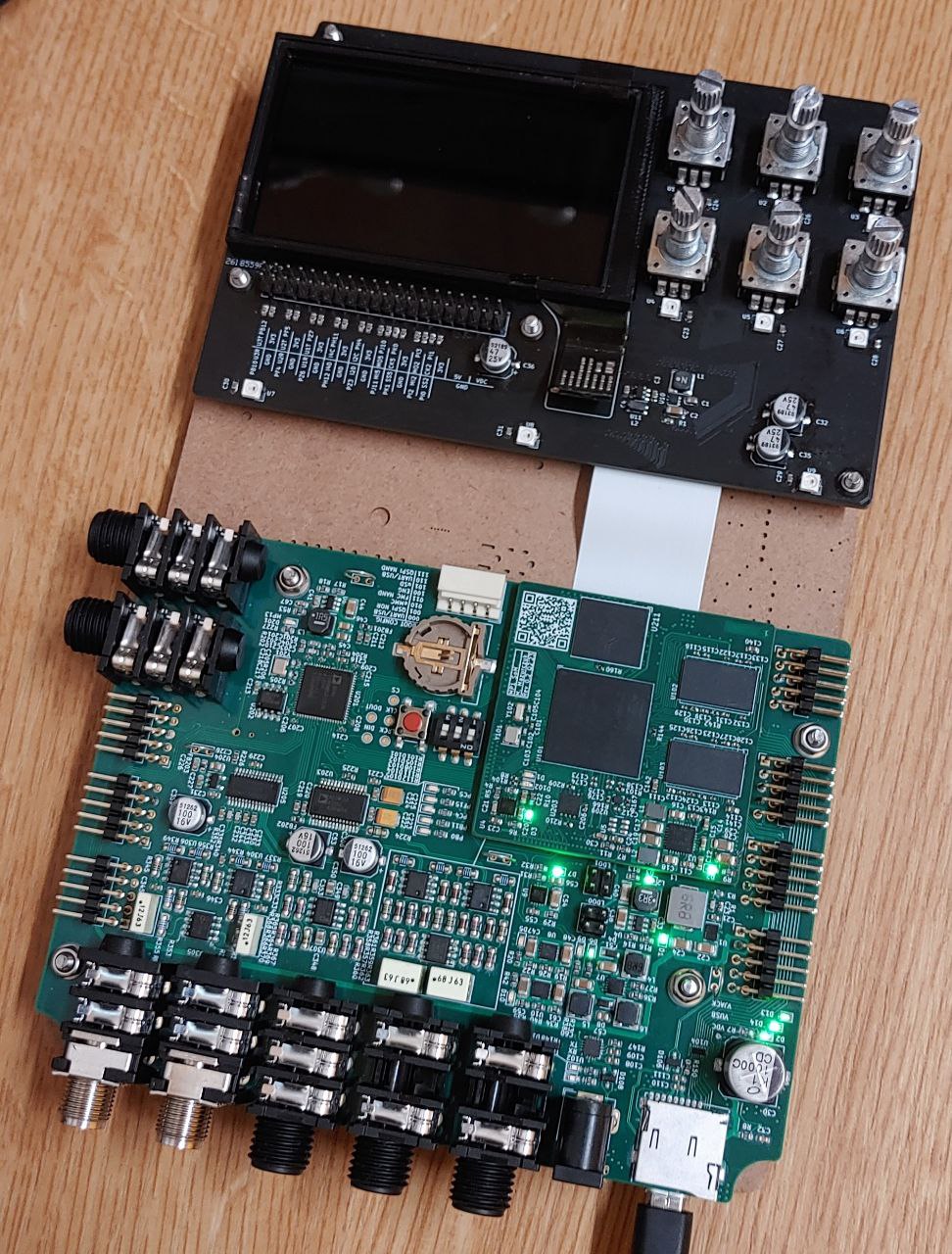
This time I have anticipated that packaging everything will be a challenge so I decided to treat the mechanical part of the design as a first class citizen. I wanted to keep the enclosure consistent with previous iterations so after downloading the 3D model from Hammond's website I went to town with trying to fit as much I/O as possible in this form-factor. After a few back-and-forth cycles I was happy with the result -- I have locked all of the components in place and continued with designing and routing the rest of the PCBs. This approach also allowed me to fully utilize available real estate and employ a layered structure. The Audio Carrier and I/O boards are connected using a pair of 50-pin ribbon cables with gaps between those two as tight as 2 mm.
PCB Overview
My audio processing system consists of three PCBs with varying levels of complexity:
- MP1 SoM (System on Module) -- the brains of the operation. The densest and most advanced board in this project
- Audio Carrier -- essentially a motherboard. Connects everything together, houses power supplies and audio circuitry
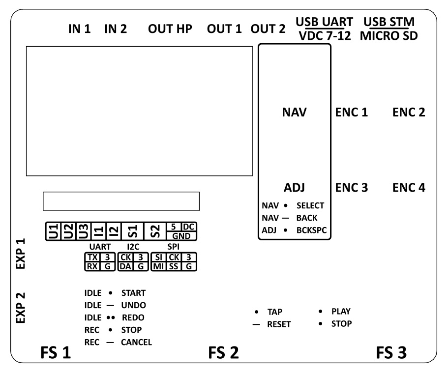
- I/O Board -- a simple, dumb, 2-layer board tasked with housing the LCD, rotary encoders, LEDs and an expansion header
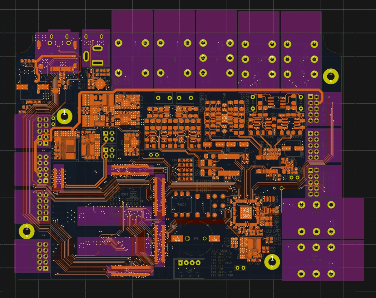
STM32MP1 System on Module
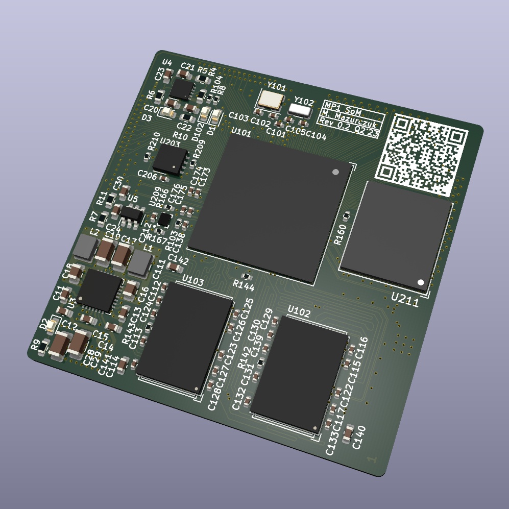
The star of the show, my most advanced PCB to date. Although low density by modern industry standards, this is still a fairly dense 8-layer PCB housing the MPU, DDR3L RAM, eMMC, some minor peripherals and relevant power supplies. Despite being the PCB that I am most proud of, it almost did not get made.
At first, I wanted to make a monolithic audio/processing PCB. Thankfully I have decided to try out this idea first by implementing the STM32MP1 MPU on a 6-layer board. This device was intended as a development platform constrained to a 100x100 mm footprint. This exercise has shown me that a monolithic system does not make much sense. There were a couple of reasons:
- Size -- the MPU subsystem ended up consuming a significant amount of space (65x65 mm) while essentially making this area inaccessible for any other signals due to complex power supply and memory layout. Going with a separate 8-layer PCB allowed me to reduce the footprint to 50x50 mm as well as has freed up space below it (essentially creating a local 12-layer area)
- Cost -- a large 6-layer board would have cost a pretty penny. Splitting the system into a small 8-layer and a large 4-layer board has cut the PCB cost in half
- Ease of Assembly -- it is essential for the solder paste to be applied as evenly as possible while working with BGA packages as there is no way to rework them after reflow (in hobbyist setting). It would be extremely hard to apply solder paste evenly over a large monolithic 140x105 mm PCB by hand. Separating this problem into a single 50x50 mm PCB greatly increased the chance of a successful paste application
- Modularity -- this approach allows me to redesign just the SoM part of the system in case I would need a more beefy CPU
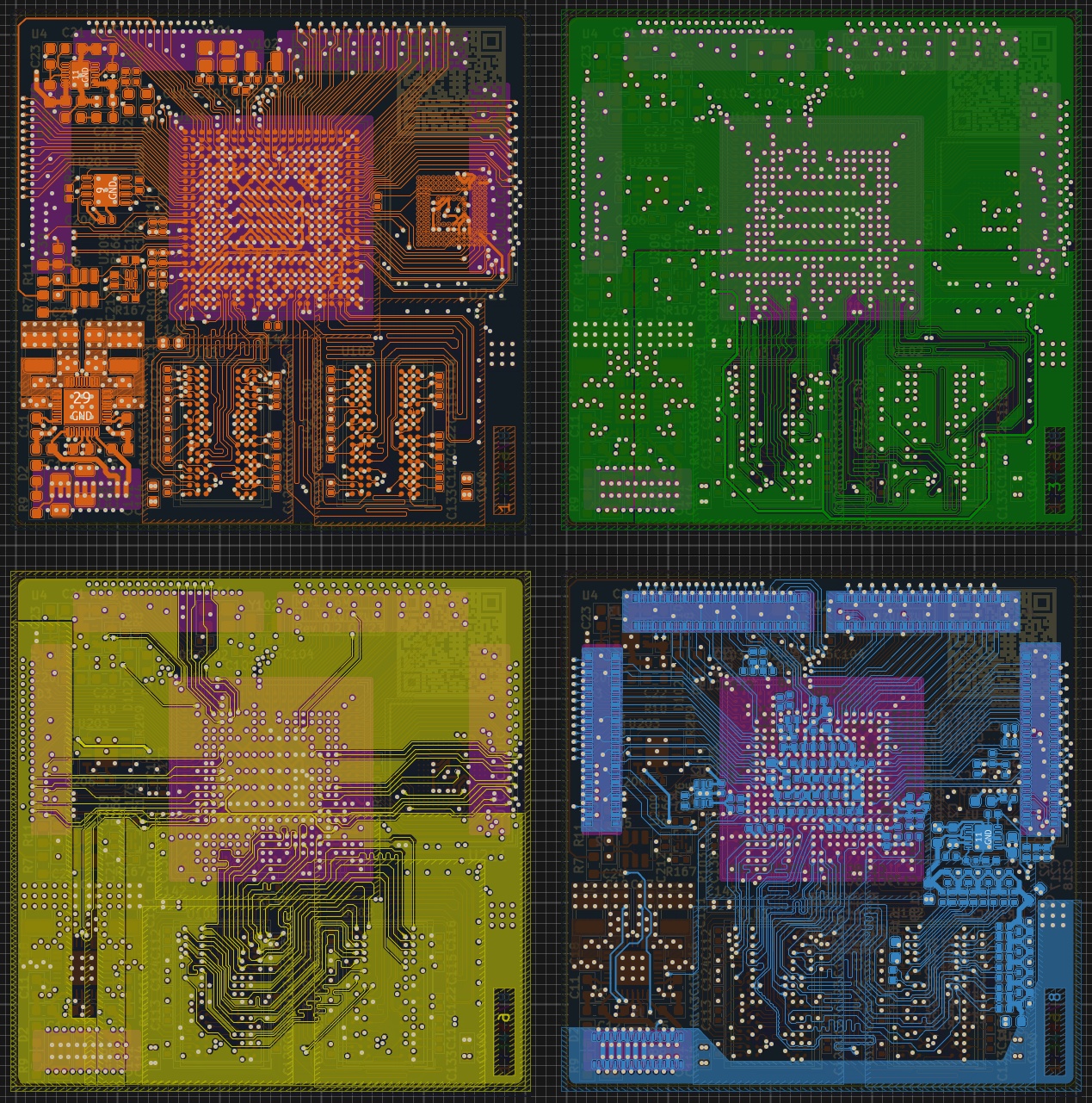
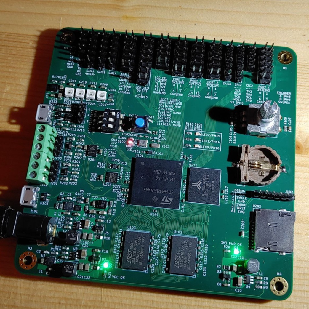
Audio Carrier
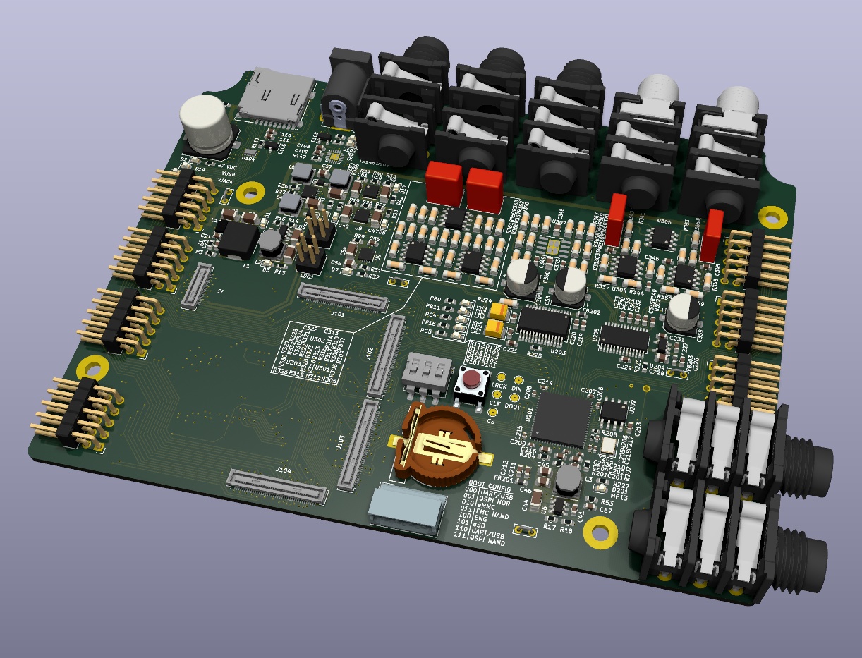
This is the largest PCB of this project measuring at 140x105 mm. It serves as a motherboard for the whole system featuring a whole range of I/O from the high-speed, high-density SoM connectors to the low-frequency expression pedal jacks. The perimeter is filled with connectors and the internal area is split into quadrants:
- Analog front end for the A/D and D/A converters
- Power supplies
- SoM, backup battery, reset and boot switches
- A/D, D/A conversion and the ADAU DSP
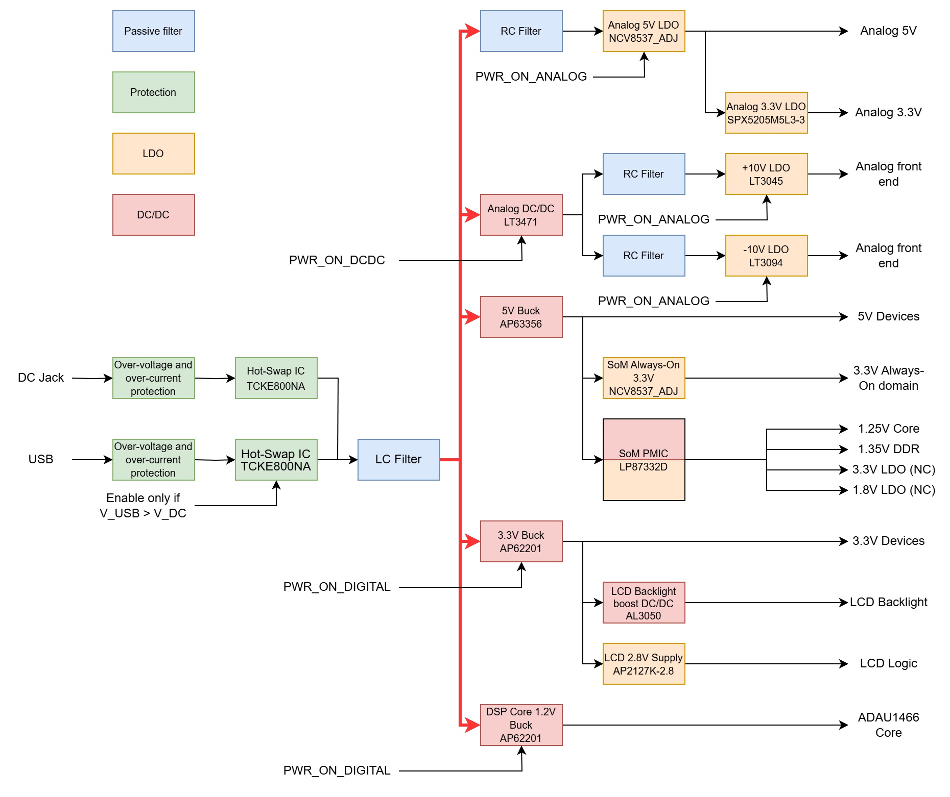
While most of the circuitry is not super inventive (mostly following reference designs with slight modifications), the power supply is quite interesting. This system features hot swappable power inputs, where you can supply the power either through one of the USB ports or a DC jack. In case of low voltage supply (less than 7 volts) the analog section will stay powered down allowing for easier development, as all you need for programming and testing your code (as long as it in not audio) is a micro USB cable. Below is the schematic of the power tree. In case a node does not have an enable signal it means that it is always active.
I/O Board
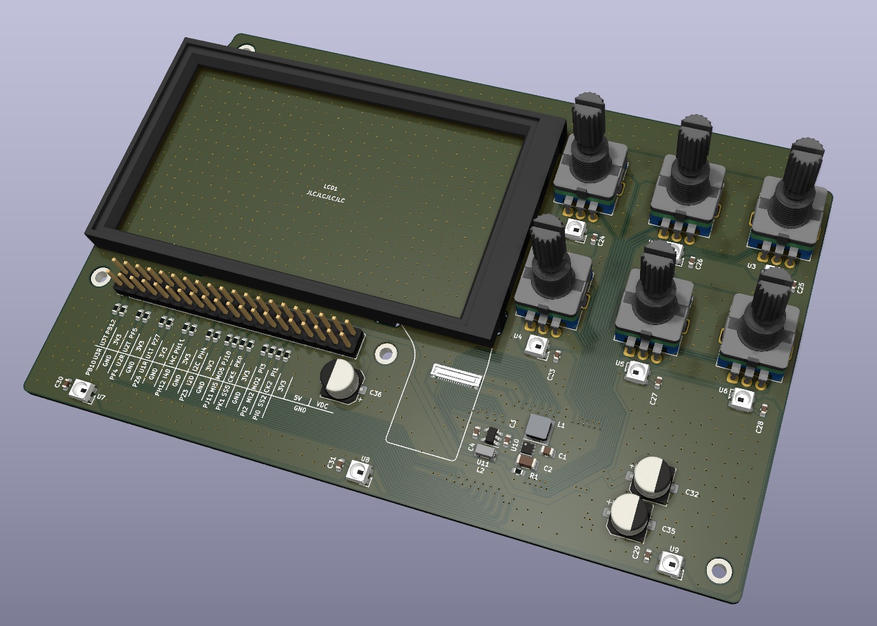
This is a simple PCB that houses all of the front panel I/O. By using ribbon cables as a connecting medium between this and the Audio Carrier PCB, the system becomes mechanically decoupled allowing for some movement between parts which leads to easier assembly and less internal stress in the structure.
Bringup, Issues, Mods
One thing you learn through experience in any engineering field is that it is super important to design prototypes not for the final use case but for ease of evaluation and experimentation. Being a hobbyist, I did not want to sink hundreds of hours into a prototype platform just to be required to redesign it to fit into my desired form factor. I chose a compromise where I support two spatial configurations:
- Folded -- to fit in the enclosure
- Butterflied -- for ease of access during bringup and debugging
Thankfully, multiple ERC, DRC and peer review sessions have paid off -- there were no critical issues with the system. The only significant problem was that I have mistakenly swapped the headphone output amplifier input polarity -- nothing a few cuts and pieces of Kynar wire cannot fix. I have also discovered that one of the digital audio expansion ports is miswired but this is a non-issue as I still have two left.
I did introduce two mods though:
- Input voltage monitoring to allow for turning the analog section on or off depending on the voltage source
- Headphone output reconfiguration to equalize the DAC load current for the positive and negative outputs
Next Steps
When it comes to what needs to be done hardware-wise, there is only one thing left -- take care of the aesthetics. I want to paint the enclosure white and add a basic descriptive faceplate.
Of course I am never fully satisfied, so I already have a growing list of modifications I would like to incorporate when I get around to designing the fifth iteration (2026? 2027?):
- The STM32MP2 series of MPUs brings a significant performance bump (2-3x) while keeping a very similar level of HW design complexity compared to the current SoM
- Power consumption and thermal management is an issue I did not anticipate -- the system as a whole consumes 6-7 W of power split evenly between the analog and digital sections. I would like to bring it down (ideally to 2-3 W range) to allow for fully-featured operation on USB power alone
So far that is it. And because I am not hitting a CPU wall just yet, I have decided to focus on audio effects development for now. After all, this is the reason why I am doing this in the first place.
Closing Words
All in all, after hundreds (thousands?) of hours of designing, debugging and programming I can honestly say that I am extremely happy with how this project turned out. I have a fully-self-built, high-performance (both in digital and analog domains) and flexible platform that I have not found the limits of yet. While each of the previous iterations had some obvious major problems, this one does not and I can finally fully focus on designing my own digital effects without having to worry about hardware capabilities. Hopefully this project will inspire someone to do something that steps outside of the usual DIY levels of complexity. I also wanted to show that such project is an iterative process -- the only way to succeed as a beginner it to design and build a rough sketch and then refine it. There is essentially zero chance to perfectly execute your vision in one shot, but by constantly iterating on your mistakes, you will approach the device you have always dreamed of. Eventually. Just to be clear -- this path is not easy but the satisfaction you get is totally worth it.
Thanks for stopping by!